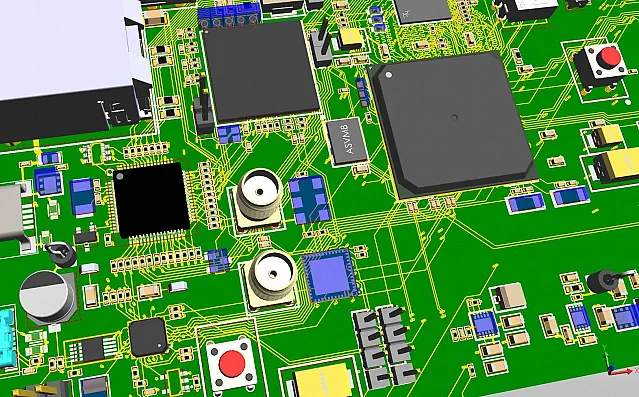
Eremex, a Russia-based electronic CAD software developer, announced the release of the 2018 version of its flagship Delta Design for designing printed circuit boards (PCB). It features 3D modeling functionality developed using modules from the C3D Toolkit of C3D Labs.
After adding the C3D Modeler geometric kernel and C3D Converter data exchange module, Eremex released Delta Design with the following new features for electronic design:
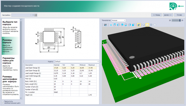
- Footprint manager now visualizes components as 3D models
- New automatic mode for associating third-party models to footprints
Delta Design 2.6 allows the use of third-party 3D models of electronic components. During the desing process, it is important to accurately orient imported models relative to the PCB footprints. The new function aligns them automatically, and so PCB designers do not need to calculate the position of the model in order to match the footprint. Designers just need to rotate the model so that it is located in the XY plane, and then the software aligns the pins automatically.
When creating new footprints through masters, there is no longer a need to associate a component 3D model. For all standard packages, 3D models are created automatically and then displayed immediately after entering parameters of the specific package from a datasheet.
Sergey Rybkin, lead developer at Eremex:
Yuri Kozulin, head of the C3D Modeler department:

“To deliver the visualization of sophisticated PCBs to Delta Design, we accelerated region operations in C3D Modeler. Regions are defined as connected domains of 2D space that are bounded by one outer and one or more internal contours. Boolean operations on such objects are performed often when working with a large number of components in a printed circuit board. As a result, our C3D Toolkit has been improved for ECAD software.”


“We requested new features in the C3D Modeler to help us to add functions to Delta Design and to visualize complex printed circuit boards. This was possible because the C3D Labs team closely cooperated with us.”